
Scanning Electron Microscope (SEM)
The Scanning Electron Microscope (SEM) is an advanced microscopic analysis technology widely used in fields such as electronic components, materials science, biology, and nanotechnology. SEM scans the surface of samples with a high-energy electron beam to generate high-resolution three-dimensional images, revealing the microstructure and composition of the sample. SEM is a powerful tool for quality control, failure analysis, and material research, providing unprecedented detail and accuracy.
Basic Principles and Importance of SEM
SEM utilizes an electron beam to scan the sample surface. The interaction between the electron beam and the sample generates secondary electrons, backscattered electrons, and characteristic X-rays. Secondary electrons are used for imaging, providing surface morphology information; backscattered electrons display atomic number contrast in the sample; characteristic X-rays are used for elemental analysis. The resolution and contrast of SEM images enable the identification of tiny structures and defects.
SEM is crucial in quality control and failure analysis. For electronic components and materials, SEM can reveal micro-defects in manufacturing processes, such as solder cracks, grain structures, and surface contamination. In nanotechnology and materials science research, SEM offers detailed observations of nanostructures, advancing the development of new materials and technologies.
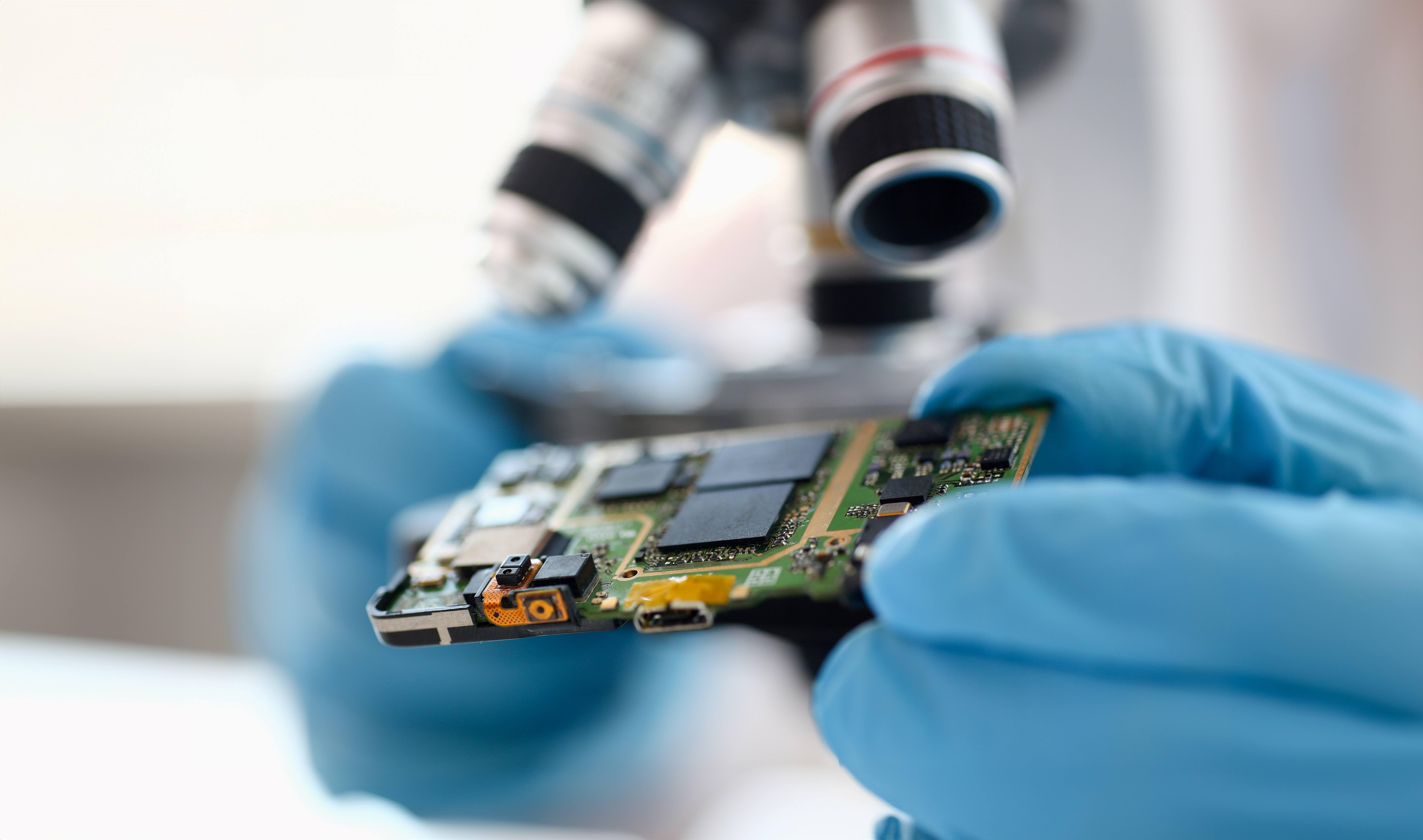
Process of SEM
Testing Preparation:
● Define analysis objectives and requirements, and select appropriate SEM settings and parameters.
● Prepare test samples, and clean and dry them to ensure optimal imaging results.
Sample Mounting:
● Fix the sample on the specimen stage to ensure stability and correct positioning.
● Load the sample in a high vacuum environment to minimize interaction between the electron beam and air molecules.
Electron Beam Scanning:
● Adjust the electron beam's acceleration voltage, probe current, and scan speed to optimize image resolution and contrast.
● Scan the sample surface point-by-point with the electron beam, collecting signals from secondary electrons and backscattered electrons.
Image Acquisition and Analysis:
● Use specialized software to process and analyze SEM images, and identify the sample's microstructures and defects.
● Conduct elemental analysis and surface composition studies, determining the sample's chemical composition through Energy Dispersive X-ray Spectroscopy (EDS).
Report Preparation and Results Interpretation:
● Thoroughly document analysis results, including images and elemental analysis data.
● Compile detailed SEM analysis reports for subsequent quality control and research references.
SEM Equipment
● Electron Gun: Generates high-energy electron beams. Common types include tungsten filament electron guns, Field Emission Guns (FEG), and cold cathode electron guns.
● Detectors: Secondary electron detectors for imaging, backscattered electron detectors for atomic number contrast, and Energy Dispersive X-ray Spectroscopy (EDS) detectors for elemental analysis.
● Microscopy Imaging System: Includes hardware and software for controlling electron beam scanning, image acquisition, and data processing.
In our laboratory, the Scanning Electron Microscope (SEM) is a crucial tool to ensure the quality and performance of electronic components and materials. Through the use of advanced SEM equipment and techniques, we provide precise and comprehensive analysis of microstructures and compositions to our customers. This not only helps identify and avoid potentially defective components but also enhances overall product reliability and market competitiveness. Our analysis services ensure customers can confidently select and use the highest quality materials and components, thereby achieving superior product performance and safety.